
Beeping out the board - Retro Challenge 2017/04
I first started with this board by pulling off the ROMs and dumping their contents. Being a m68k CPU generally the ROMs are split into odd and even byte streams, and in order to dissassemble them the two ROM images need to be interleaved again. I achieved this with a little bit of python:
#!/usr/bin/python3

import os
import argparse

parser = argparse.ArgumentParser()
parser.add_argument("odd_file")
parser.add_argument("even_file")
parser.add_argument("output")
args = parser.parse_args()

with open(args.output, 'wb') as out:
  with open(args.odd_file, 'rb') as odd:
    with open(args.even_file, 'rb') as even:

      odd.seek(0, os.SEEK_END)
      odd_size = odd.tell()

      even.seek(0, os.SEEK_END)
      even_size = even.tell()

      if (odd_size != even_size):
        exit("ROM images aren't the same size!")

      odd.seek(0)
      even.seek(0)

      for c in range(0, odd_size):
        odd.seek(c)
        even.seek(c)

        out.write(odd.read(1))
        out.write(even.read(1))
ROMing around like it’s 1995
I took the two ROM images I dumped and merged them back together using the following:
$ merge.py rom_odd.bin rom_even.bin rom_out.bin
After verifying the rom_out.bin using objdump for the m86k I knew I was on my way.
$ m68k-linux-gnu-objdump --disassemble-all --target=binary --architecture=m68k --start-address=0x00 rom_out.bin
This gave me the disassembled output of the m68k ROM image:
rom_out.bin:     file format binary


Disassembly of section .data:

00000000 <.data>:
       0:	0002 0ff0      	orib #-16,%d2
       4:	0000 0400      	orib #0,%d0

[SNIP]
The first value is the preset value the CPU uses for the SP (stack pointer). So it looks like it’s up in 0x20000 address space. That’s a good start, looks like some RAM is up around 0x20000.
The second address is the init jump point, so the first instruction the CPU will load is at location 0x400.
The stuff you see in ROM dumps …
Further digging through the assembly and looking at hex dumps you can start to see strings (even some funny stuff) and loops testing devices and memory etc.
00009140: 3131 2100 2a21 3132 2100 5041 5353 0053  11!.*!12!.PASS.S
00009150: 454e 4420 434f 4d4d 414e 4400 5345 4e44  END COMMAND.SEND
00009160: 2053 5452 494e 4700 5055 5348 0056 414c   STRING.PUSH.VAL
00009170: 5545 204f 4600 4445 5649 4345 2053 5441  UE OF.DEVICE STA
00009180: 5455 5300 5245 4345 4956 4520 5052 4f47  TUS.RECEIVE PROG
00009190: 5241 4d00 4841 5645 2050 524f 4752 414d  RAM.HAVE PROGRAM
000091a0: 0053 484f 5720 4445 5649 4345 0043 4f4d  .SHOW DEVICE.COM
000091b0: 5041 5245 2044 4556 4943 4500 5348 4f57  PARE DEVICE.SHOW
000091c0: 2049 4e50 5554 204f 4e00 5348 4f57 2049   INPUT ON.SHOW I
000091d0: 4e50 5554 204f 4646 0041 4d58 2042 5547  NPUT OFF.AMX BUG
000091e0: 003f 0048 454c 5000 4441 5445 0054 494d  .?.HELP.DATE.TIM
000091f0: 4500 5345 5420 4441 5445 0053 4554 2054  E.SET DATE.SET T
00009200: 494d 4500 5645 5253 494f 4e00 4d45 4d4f  IME.VERSION.MEMO
00009210: 5259 0053 4c4f 5400 4841 5645 2043 4f4e  RY.SLOT.HAVE CON
00009220: 5452 4f4c 0053 5953 5445 4d20 5245 5345  TROL.SYSTEM RESE
00009230: 5400 4543 484f 204f 4e00 4543 484f 204f  T.ECHO ON.ECHO O
00009240: 4646 0053 4849 5400 4655 434b 0048 454c  FF.SHIT.FUCK.HEL
00009250: 4c4f 003e 004f 4b00 434f 4e4e 4543 5400  LO.>.OK.CONNECT.
00009260: 5249 4e47 0043 4152 5249 4552 0045 5252  RING.CARRIER.ERR
00009270: 4f52 0044 4941 4c54 4f4e 4500 4255 5359  OR.DIALTONE.BUSY
00009280: 0000 4e56 fffe 422e ffff 4a39 0002 140b  ..NV..B...J9....
00009290: 6712 7000 1039 0002 140b 41f9 0002 140c  g.p..9....A.....
Beep, beep, beeeeeeeeeep …
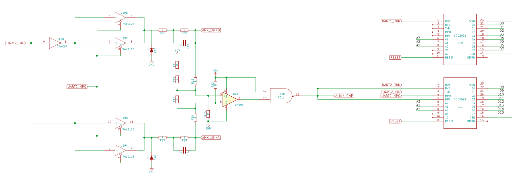
After much looking through the code I had some good ideas where things were but I still didn’t fully understand the address map of the CPU and what devices were going where. So being all DIP packages and only a dual layer board I set out with my Fluke 87 and my pointest of pointy probes and started beeping out traces on the board to get a true account of where all the devices are and what they do.
I start building up a picture in KiCad of the schematic. Not taking values of components etc, but just the general connections so that many things can become much clearer. I first tackled the address decoding.
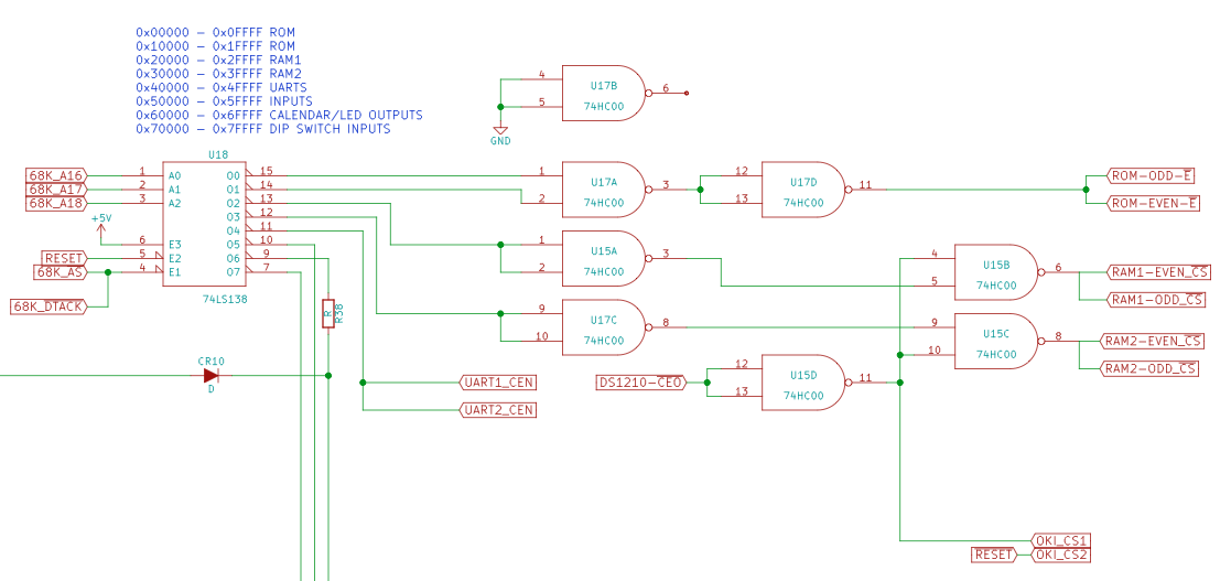
So after a lot of beeping and probing I got the address map out:
| 0x00000       | ROM                    |
| 0x10000       | ROM (addr alias?)      |
| 0x20000       | RAM BANK 1             |
| 0x30000       | RAM BANK 2             |
| 0x40000       | UARTs (2 x SCC2691)    |
| 0x50000       | INPUTs via a 74LS373   |
| 0x60000       | OUTPUTs via a 74LS259  |
| 0x70000       | INPUT via a 74LS373    |
The first INPUT and OUTPUT addresses are related to the OKI M5832 clock calendar chips 4 bit I/O bus and control lines, and the on-board green status LED. So that’s a good start.
Need to understand the UARTs a little better, one is standard RS232 the other is a weird RS485 like interface (called AXLink in AMX speak).
Anyway, that’s all for today. I’ll crack on with more tomorrow!

Comments