
After the UV fiasco I’ve finally managed to get around the issue. I did that by ditching EPROMs and instead replaced them with EEPROMs!
Rummaging around in the shed I found two other cards from the system this controller was in originally. They were for controlling infrared devices and what not and used a M68HC11 CPU. They had 27C64 EPROMs and 28C64s EEPROM each.
My guess is that rather than adding battery backed up RAM on these smaller cards, AMX opted just to use the 28C64 as SRAM since the write performance etc of them are pretty good. These smaller cards really didn’t store much other than configuration data and they would’ve just used the internal 768 bytes of RAM on chip and just set the 28C64 up as an external 8KB of non-volatile RAM.
Anyway, I found them and thought “Hmmm a blinking LED doesn’t need 64KBs (2x32KB) of ROM to work, 16KBs (2x8KB) should be ample”. The only real issue I had was that I only had two and they were from different manufacturers. I wasn’t sure if this would cause an issue or not but I figured it would be worth a try.
A try …
The 28C64s are basically almost pin compatible with the 27C256s (obviously missing the two additional address lines.
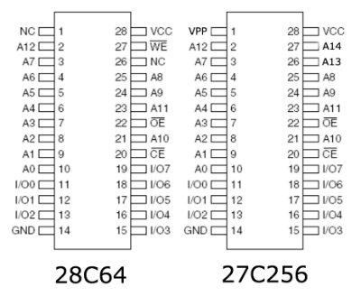
So apart from A14, A13 and the VPP signal these would plug straight in. Woo hoo I was thinking, this’ll be easy!
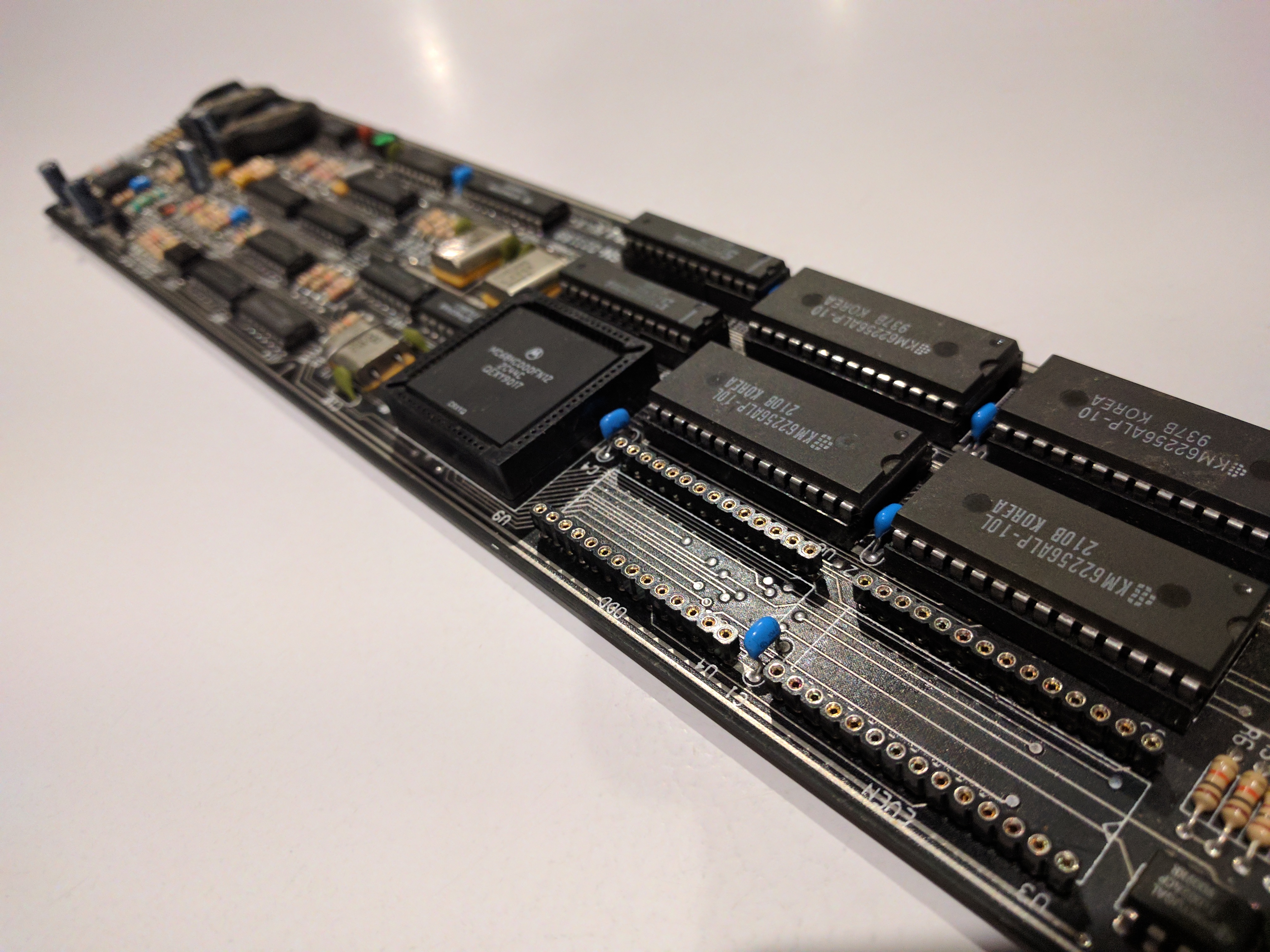
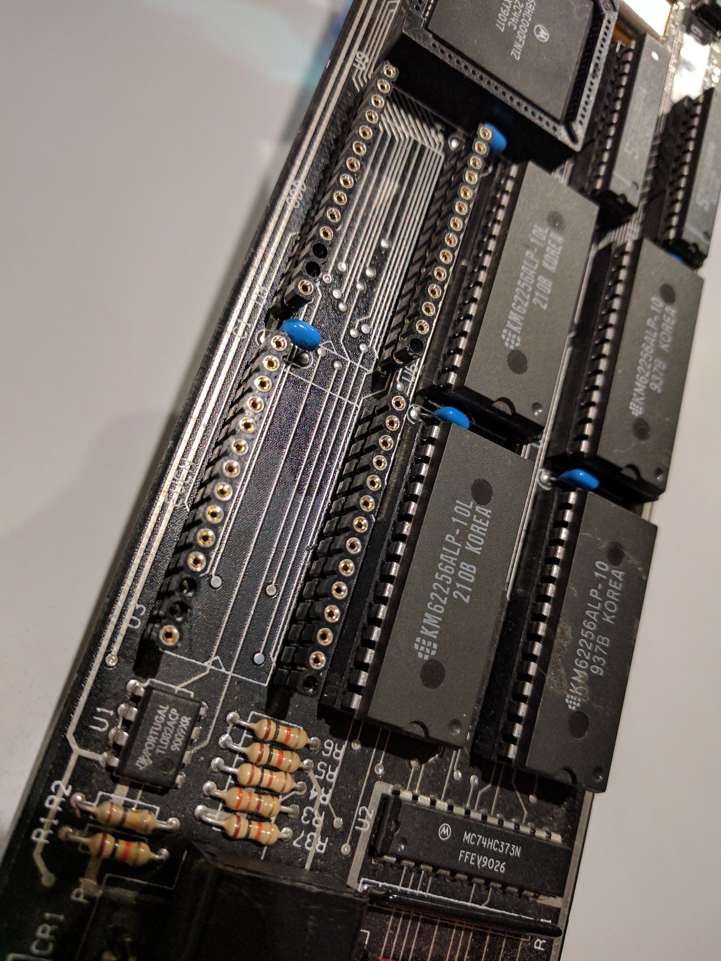
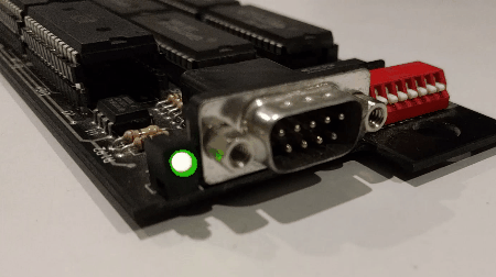
I set to work. I wanted to replace the crappy single leaf sockets that are on this board, but I wasn’t willing to do all of them in one hit. The PCB traces on the thicker tracks have started that weird bubbling/lifting thing that things of this vintage start to do. I figured it would be safer if I just did one set at a time. So I carefully desoldered the two sockets and replaced them with machine pin sockets…
It was at this time that I noticed pin 1 on these sockets had traces. Given these are the VPP lines I thought that was strange. It turns out they’re actually connected to A16! This isn’t a problem (yet) as the VPP lines require high voltage to do anything.
The solution I came up with to make the 28C64s work without their write enable line being connected to A14 was to add another layer of machine pins with the sockets missing.
I opted to pull out the VPP, A13 and A14 pins just to make sure. I then programmed my blink routine into the two mismatched 28C64s and expected great things to happen… And they did… briefly…
THE LED BLINKED!… sometimes.
After all the hassle with the EPROMS and UV light etc I finally had the little LED blink. The only issue was that it wouldn’t do it consistently. Sometimes it would blink 4 or 5 times then stop, other times it would blink once and stay on, and others it just wouldn’t blink at all. :(
I started to suspect that possibly different timings with the EEPROMs vendors and that the CPU was only sometimes getting it’s stars to align well enough for the LED to blink for a few cycles etc before it got all jammed up. I wasn’t too disappointed as I knew my element14 delivery was arriving in the morning with my new AT28C256’s and the fact I got the board to do anything was a total win in my book at this point.
I posted on twitter about my success and went to bed late, trying not to disturb my lovely wife once again.
Something fishy is going on.
Through my following working day I kept being suspicious of the timing conclusion I’d drawn myself into. It was odd that the CPU would process hundreds of thousands of instruction reads from these EEPROMs inside the delay loop code before “magically” the timing of the EEPROMs would became an issue and ruined the whole thing. That started to sound very very unlikely to me. It just didn’t make sense.
I then started thinking about the code, and how the interrupt and error vectors where not set correctly in the early part of the ROM code. So if the CPU had an external interrupt triggered by some of the other uninitialized hardware, the CPU could be falling into an ISR that didn’t exist and lock up.
This started to sound more and more likely to me, so once I finished work for the day I set about properly configuring the interrupt vector table and cleaning up my horrible testing code.
I wanted the code to be relocatable and the vector table be properly configured using a linker script so that I can link up a bunch of objects and have the magic of linking work with me rather than it just being a dumb copy-it-here type deal.
Building the code environment.
https://github.com/alangarf/amx_axc_m68k
After much frustration trying to figure out why ld was overwriting my new
.vector section and my general lack of understanding of a lot of what the
linker does I enlisted the help of my dear friend
Niels to help point me in the right direction.
Together we figured out my .section in my assembly code didn’t have the right
flags set so ld wasn’t loading the .vector section into the output. Rightly
so because it thought it didn’t have to. After we figured that out the vectors
where properly being set, and I had a workable development setup to continue on
with.
I later discovered that objcopy also can generate interleaved binary files
just for the purpose of creating ROM files for systems like this one. So rather
than using some dodgy python I wrote quickly to split the resulting binary ROM
image in half, I simply made objcopy create an even and an odd ROM
image!
Suitably chuffed with myself at this point.
AT28C256s arrive!
Again, element14 in Sydney amaze me. My AT28C256s were ordered at 5:30PM the day before, and arrived at my door in country NSW Australia by lunch time the next day. I’m about 5 hours drive away from their warehouse (I used to live near their warehouse and boy it was useful), so it’s truly amazing how quickly I can get parts from them.
Anyway, deciding for a quick win I didn’t bother creating a pin swapping socket for these new chips. I figured I’d just use only the first 8KB of them and drop them into the existing sockets I had for the 28C64s.
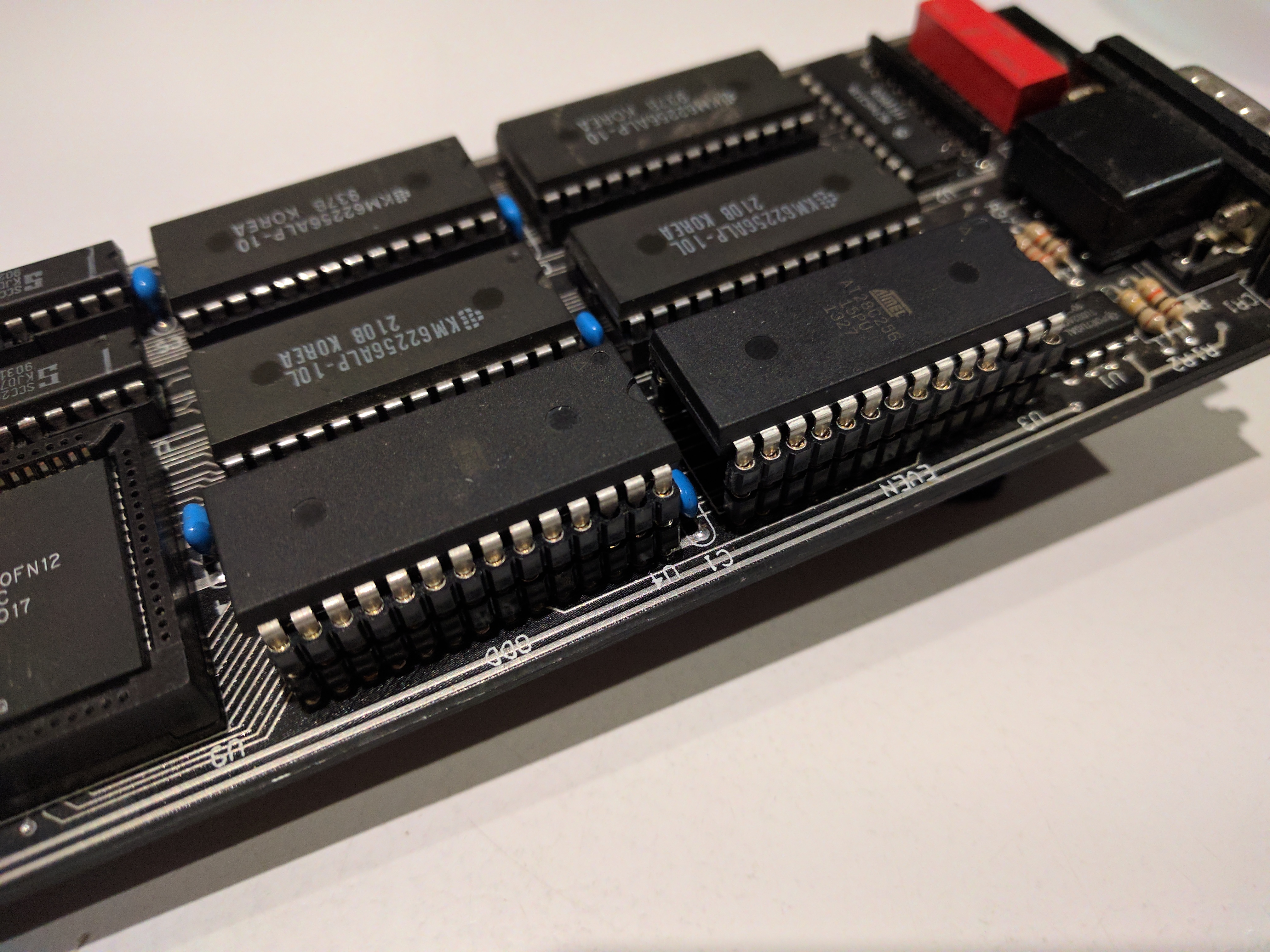
I realized after plugging them in that had I not removed the VPP lines from these sockets that I would’ve connected A16 to the A14 pin on these EEPROMs, which would’ve allowed for 16KBs of ROM split across 0x0000 -> 0x3FFF and 0x8000 -> 0xBFFF.
But more importantly when I do properly do the pin swap to make these into a continuous 64KB address space the write enable pin would end up at the VPP position which now I know has A16 attached to it!
This could’ve had all sorts of weird consequences had I not known that now!
So did it work?
I powered up the board with the new EEPROMs and the updated code and success it blinked perfectly, a nice solid consistent blink…
… until I lifted the board.
UGH, you’re kidding me.
It seems like the issue I had with the other 28C64s wasn’t timing or bad code, it was a plain and simple dry joint somewhere on this board causing all the issues. :(
I mean expecting a 27 year old board that spent at least 10 years bouncing around my garage to have no damage after all this time probably was a little naive.
When testing the manufacturers firmware via a serial terminal I remember noticing initially that sometimes the board wouldn’t boot properly or it would crash sometimes. But even then I attributed this to a bad serial lead or the shitty terminal emulator I had on my Windows machine in the shed.
So, now I have a treasure hunt on my hands. Is it a bad solder joint, or a cracked trace somewhere on the board. I’m going to start with resolding all the connections first, then I’ll start looking more closely at the traces. The main issue I have is that a lot of the traces are hidden under sockets and immovable devices so that could be fun. BUT at least now I have a working board with a known issue. If I giggle the board just so I can make it work reliably. So that’s a win in my book!
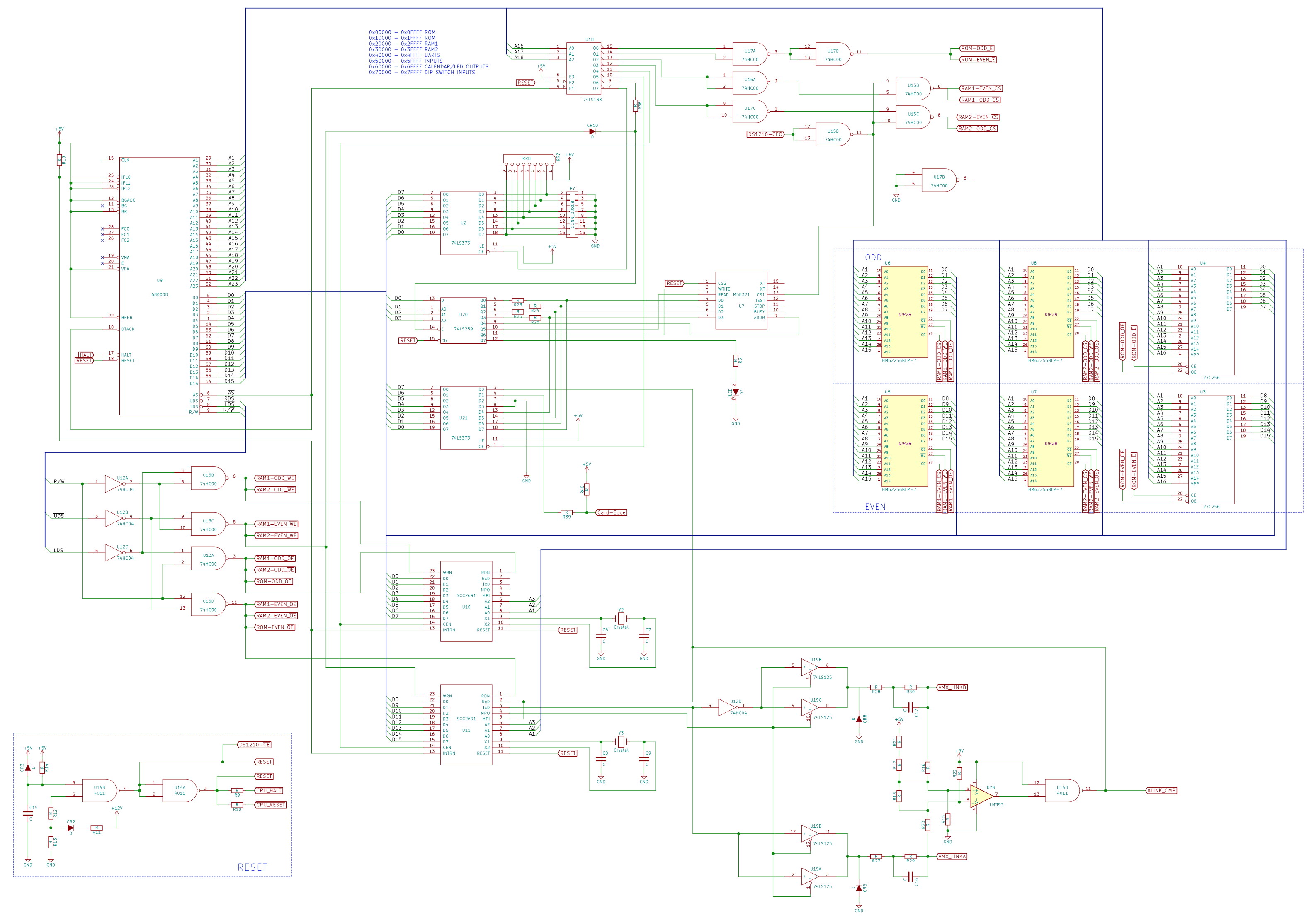
What else have you done though, what about that schema?
Yeah I’ve updated the schematic some more, apart from the level conversion of the RS232 port I’ve got the entire schematic done now. You can get the KiCAD files from: https://github.com/alangarf/amx_axc_kicad.
Is that all?
Yeah I think that’ll do for today. :)

Comments